What we do
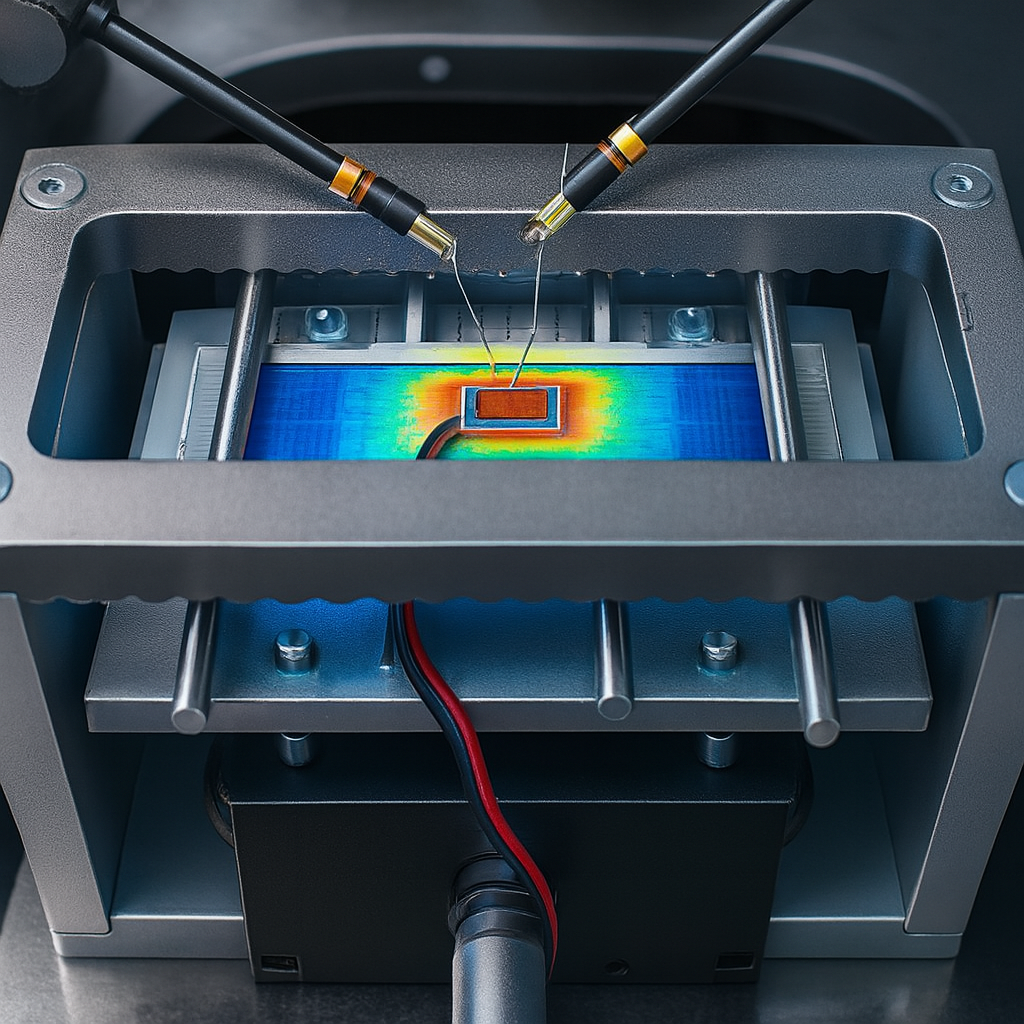
Strain may be a pain !
During our ASIC design activities, we occasionally faced unexpected circuit behaviors that were extremely difficult to diagnose.
One recurring issue was mechanical strain, induced by packaging processes but also by temperature cycles during operation (cryo or high temperature applications), which affected the stability of bandgap references and sensors.
To address this, we developed an integrated strain sensor IP capable of measuring local two-dimensional strain on a silicon die.
This technology enables real-time monitoring and mapping of mechanical stress across the silicon surface. It can be used both as a diagnostic tool during development or operation and as a mean to optimize manufacturing processes, reducing variability and improving the reliability of sensitive analog and sensing circuits.
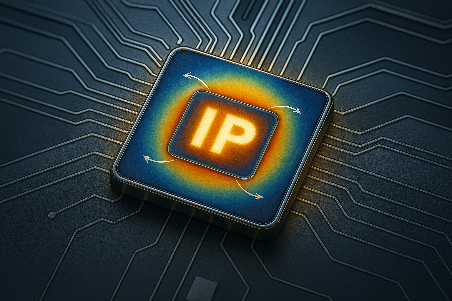
IP blocks
Detect local strain at the transistor level
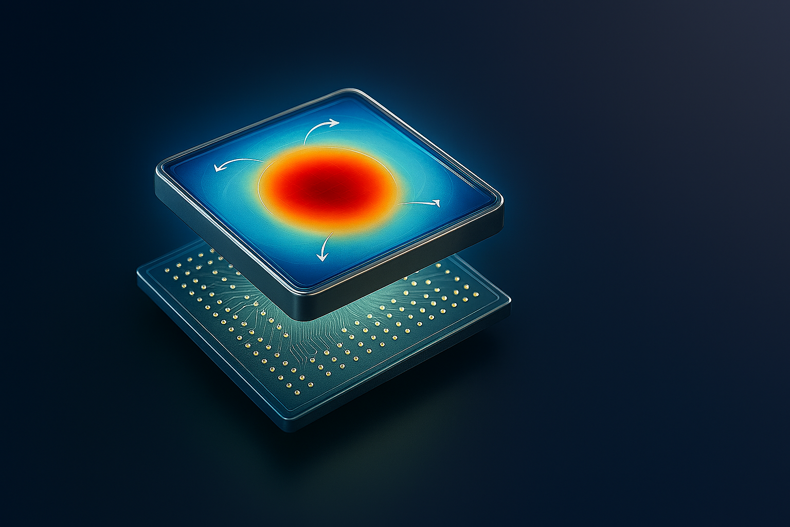
Chiplets
Visualize die deformation within advanced multi-chip systems
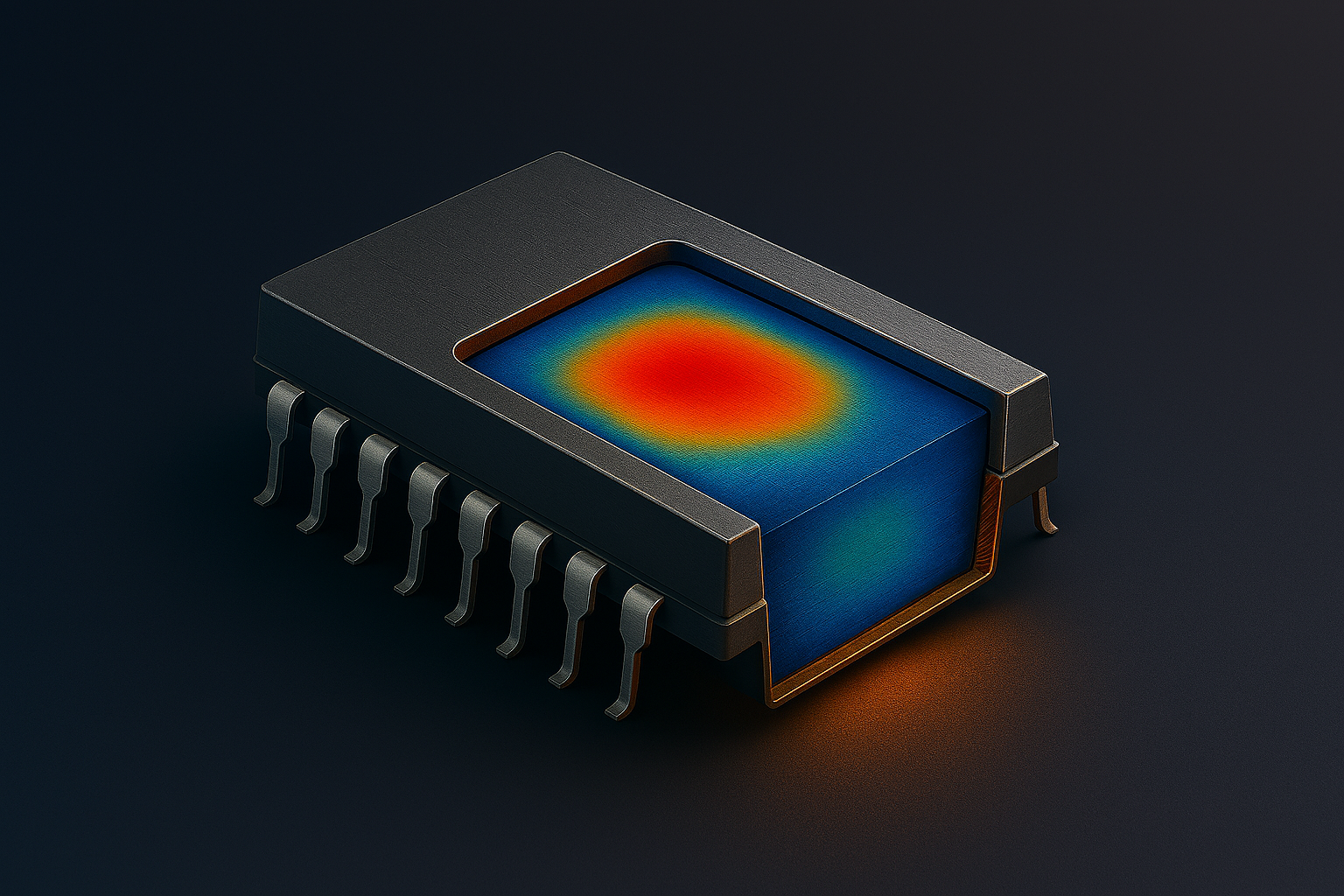
Packaging strain study
Understand and optimize package-induced stress
portfolio
Design service projects
Our team has a significant experience in analog IC design for some major companies dealing with spatial, automotive, oil & gas and industrial applications, dealing with analog to digital conversion, sensor interfacing, power management units, ultra low power references, high speed IOs, PLLs and SerDes.
We also have experience dealing with complex packaging (gas sensing, System-in-Package, signal integrity verification, cost optimization), with characterization, qualification and production of complex mixed-signal ASICs.
Please find below some relevant projects.

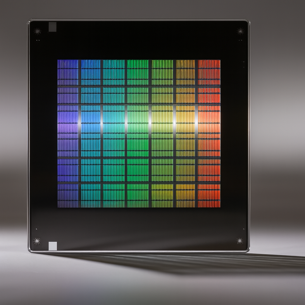
Gas sensing platform
We developed a complete gas sensing platform for a start-up company, bringing together advanced sensor design and custom electronics in a single, compact solution.
The system integrates a low-cost transducer chip featuring a 16-pixel array for multi-gas detection, coupled with an ultra low-power mixed-signal front-end that ensures precise signal conditioning, conversion and transmission via I²C. Both components are assembled within a custom package, and optimized for manufacturability, testability, scalability, and easy integration into future product lines.
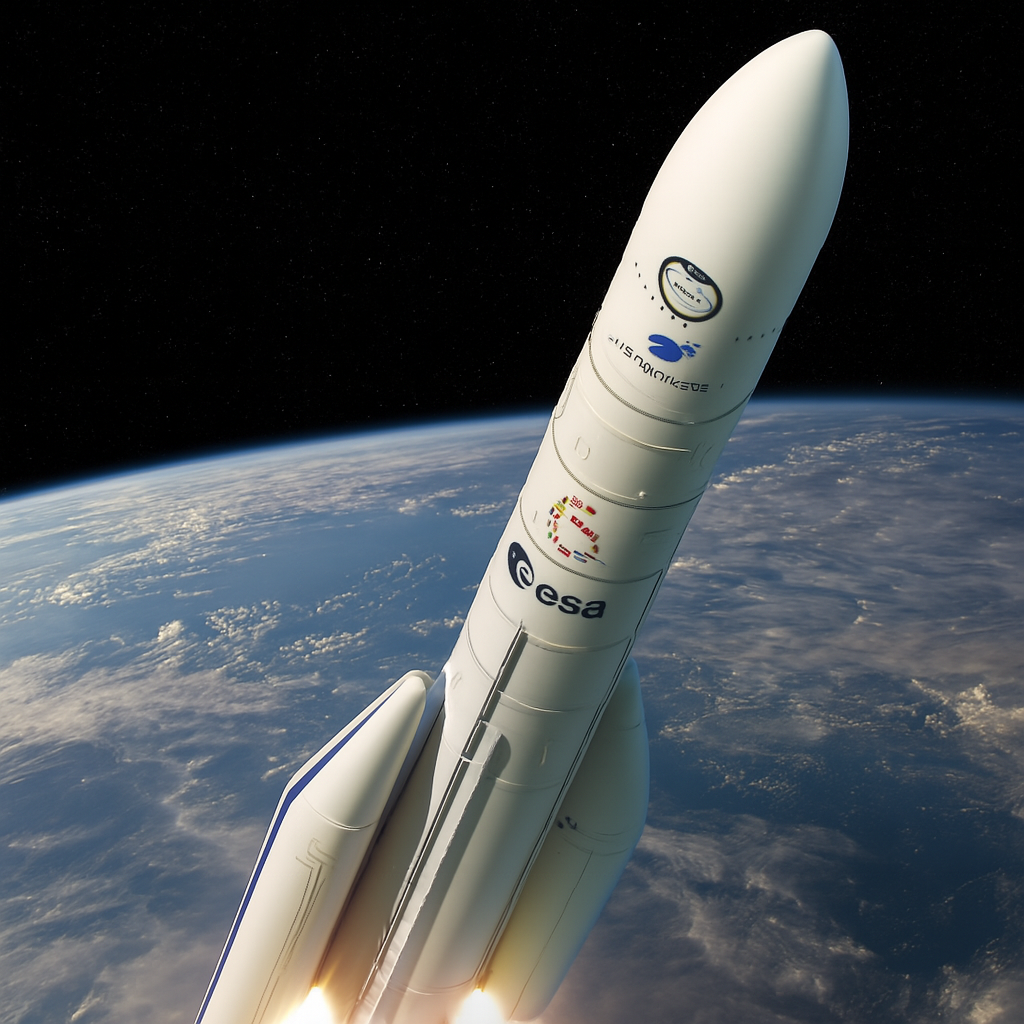
Radiation hard analog and digital library
We played a central role in the development and qualification of the DARE technology libraries for the European Space Agency (ESA).
Our contribution covered the device modelization, the design and characterization of these radiation-hardened platforms, ensuring their robustness and long-term reliability under harsh space conditions. We were directly involved in the creation of both the analog and digital foundations of the DARE ecosystem (from precision analog building blocks to optimized digital standard cells) across several technology generations, including DARE 180, DARE 65, and DARE 22.
This work laid the groundwork for high-performance, radiation-tolerant ASICs now used in a wide range of ESA missions.

Power management unit for automotive
We provided an automotive-grade Power Management Unit (PMU), on TSMC 28 nm technology, managing multiple power domains and operating modes — test, deep-sleep, sleep, and active. It integrates on-chip regulators and references, and voltage and current monitoring for efficient and reliable power sequencing.
Designed for automotive environments, it ensures robust operation under wide temperature and safety constraints, with features such as fault detection, watchdog supervision, and programmable thresholds power-on-reset (POR) and voltage monitors. Combining high integration, low power, and proven reliability, this PMU provides a compact and scalable solution for next-generation automotive systems.
High-density electron beam deflector
We designed a high-density electron beam deflector in TSMC 28 nm. Organized as a scalable matrix it enables precise, high-speed engraving of photolithography masks. Each deflection channel in the array is optimized for minimal crosstalk and fast switching, ensuring accurate beam placement across the full matrix.
This design combines high density with manufacturability, making it ideal for mask writing and other applications requiring fine-resolution electron beam control.
Management team

Guillaume Pollissard
Founder
He holds a PhD in engineering from the Université catholique de Louvain and brings about 20 years of experience in mixed-signal integrated circuit design.
Throughout his career, he has led advanced developments in sensor interfaces, analog front-ends, and low-power architectures.
Before joining us, he served as VP of Engineering at VOCSens, where he oversaw the design and industrialization of cutting-edge environmental sensing solutions.

Anne-Emmanuelle Mevel
Management Assistant
Behind the scenes, she ensures that everything runs smoothly, from daily operations to HR and team logistics. With a strong sense of organization and attention to detail, she keeps communication flowing between the team, clients, and partners.
Her efficiency and reliability make her a cornerstone of our company’s day-to-day activity, allowing engineers to focus fully on innovation and execution.
Join us now !
We are looking for skilled engineers to join us shape the future of advanced technologies.
Whether you’re passionate about semiconductors, embedded systems, or precision engineering, your expertise belongs here.
Join a team where curiosity is valued, rigor is respected, and impact is real.
Contact us
Whether you’re curious about our technologies, interested in joining the team, or simply want to start a conversation, we’d love to hear from you.
Fill out the form and we’ll get back to you shortly.